Mosaic - Programmable Neural Processing Unit
Mosaic is a custom 8-bit neural processing unit inspired by NVIDIA's open-source NVDLA architecture. I'm building it from the ground up to work through how AI hardware handles computation, memory movement, and inference.
architecture
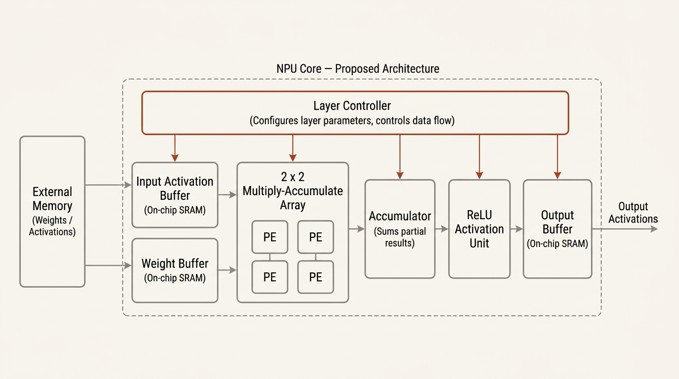
The intended datapath starts with local buffers for input activations, the values moving through a neural network, and weights, the learned coefficients used to transform them. Both feed a 2×2 array of multiply-accumulate processing elements, which multiply pairs of values and add the products into running sums.
A programmable layer controller will sequence the work. An accumulator will collect partial results, then a ReLU activation unit will replace negative values with zero before they reach the output buffer. This is the proposed structure, not a completed hardware implementation.
memory efficiency
A major part of the project is comparing on-chip reuse and intermediate-result forwarding against designs that need additional memory transfers. Reuse keeps values nearby for multiple operations; forwarding passes an intermediate result directly to the next operation instead of writing it out and reading it back.
I'll measure execution cycles, memory accesses, and data movement to see what those choices change. There are no measured performance results to report yet.
verification
I'm using SystemVerilog for the register-transfer-level (RTL) design, which describes how values move between registers each clock cycle. Python reference models will compute expected outputs so I can check the hardware's arithmetic and layer execution. The work combines computer architecture with digital verification, first for individual components and then for the integrated accelerator.
development plan
The project is in progress, with a 70-day plan that starts with learning SystemVerilog and designing individual hardware components. From there, the plan moves into integrating the accelerator, running neural network inference workloads, and evaluating performance and memory efficiency. Deploying the design on an FPGA is a stretch goal, not a committed deliverable.
development record
The architecture diagram above is conceptual. This section will hold hardware diagrams, simulation waveforms, and verification results as they become available. Performance graphs will follow measured runs; there are no waveforms, verification results, or performance graphs posted yet.