Adjustable AC/DC Power Converter
I built an adjustable AC/DC power supply from a 120 V AC wall outlet, finishing at roughly 0–20 V of adjustable output. The central problem was making an adjustable voltage source hold its output when a load is connected — solved with a MOSFET source-follower buffer, then verified with a multimeter and oscilloscope across several load resistances.
transformer + AC measurements
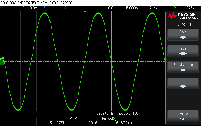
I soldered the power connector onto a prototype board for a 120 V to 24 V AC wall transformer. Using a function generator and oscilloscope, I tested its response at frequencies from 10 Hz to 1 MHz.
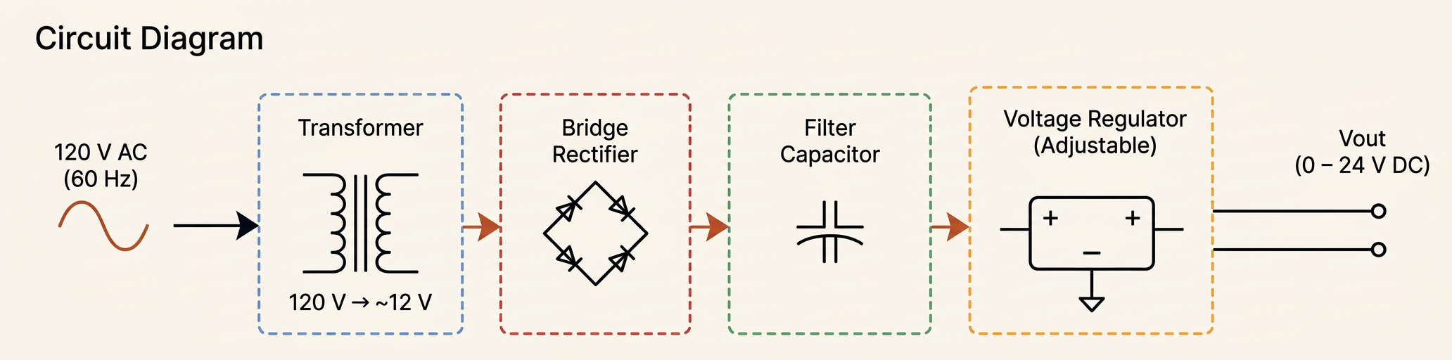
At 60 Hz, a 10 V peak-to-peak sinusoidal input produced a 4.62 V peak-to-peak output: a measured ratio of about 2.16:1 under that test setup, separate from the transformer's nominal 120 V to 24 V rating.
full-wave bridge rectifier
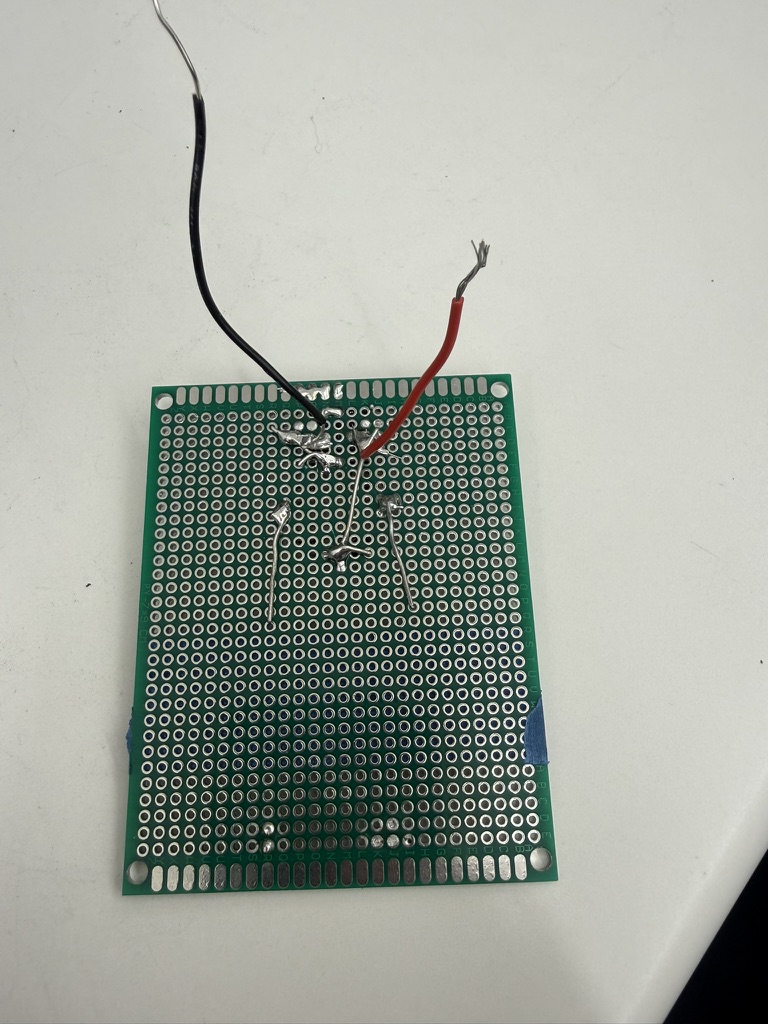
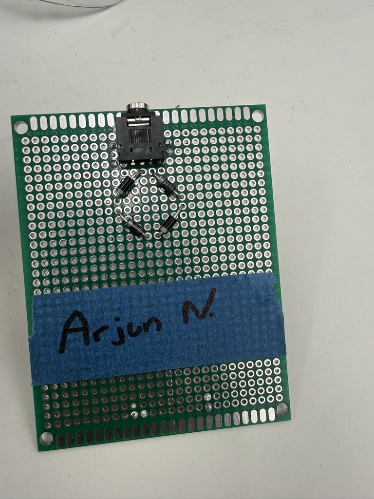
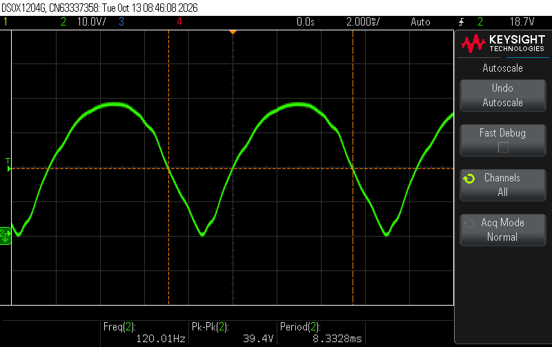
I soldered four 1N4002 silicon diodes into a bridge so both halves of the AC waveform produce the same output polarity. With a 10 kΩ load, the oscilloscope recorded 120.01 Hz, an 8.3328 ms period, and 39.4 V peak-to-peak. The roughly 120 Hz output comes from rectifying both halves of the 60 Hz input.
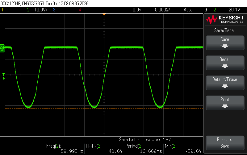
Across an individual diode, I measured a maximum forward voltage of approximately 1.0 V and a peak reverse voltage of 39.6 V.
capacitor filtering
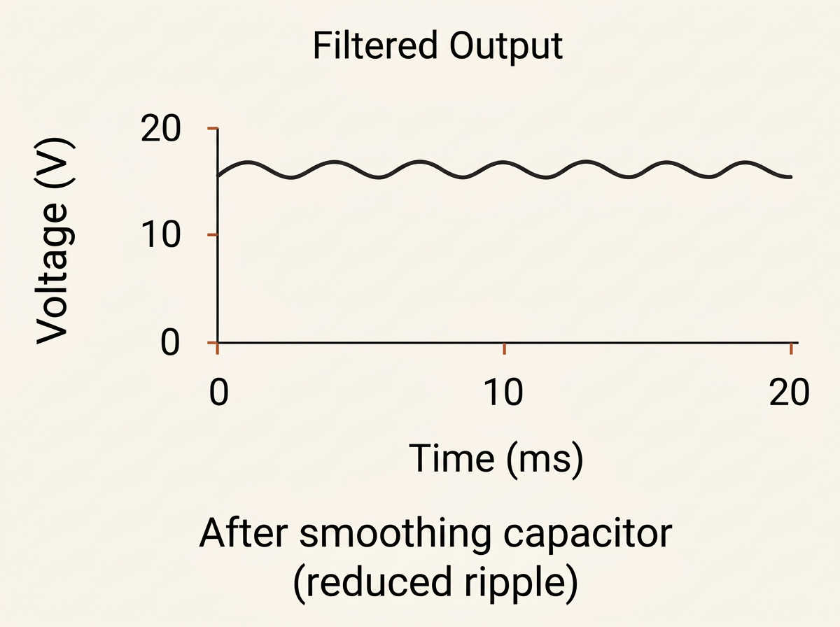
I added a 1000 µF capacitor across the rectifier output to store charge between waveform peaks and reduce ripple. I checked its polarity, discharged it safely before modifying the circuit, and examined the output with the oscilloscope.
I've also worked through how capacitance and load resistance affect ripple — the tradeoff that drove the capacitor choice and, later, the output buffer.
Zener regulation + adjustable output
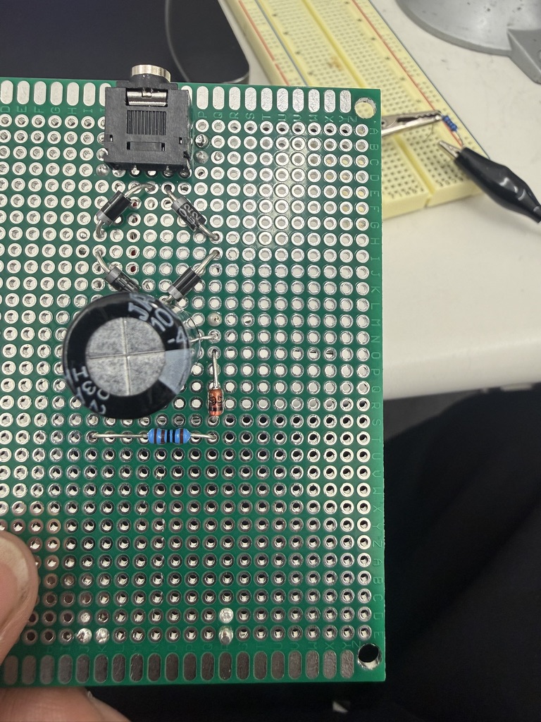
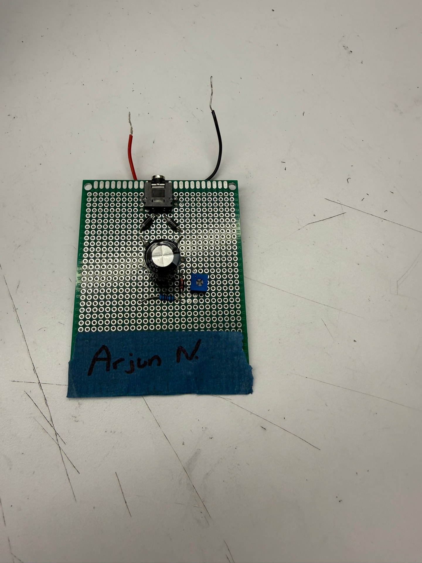
With a nominal 24 V DC supply established, I added a 24 V Zener diode and a 1 kΩ series resistor, then integrated a 10 kΩ potentiometer as a voltage divider so the wiper position sets the output voltage.
The limitation was load regulation. The potentiometer made the voltage adjustable, but its relatively high Thévenin resistance meant a low-resistance load pulled the output voltage down — the supply couldn't hold its setpoint once it had to deliver real current.
MOSFET output buffer
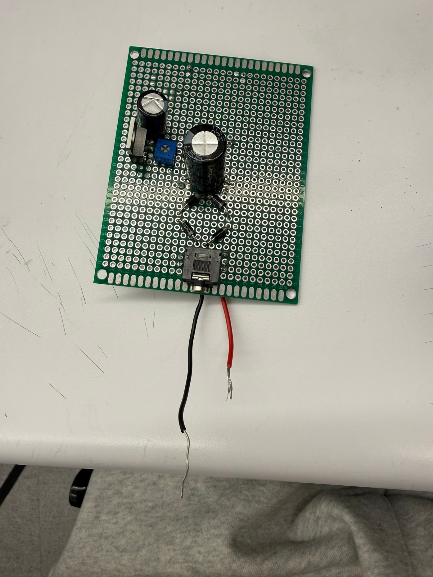
To fix the load regulation problem, I added an IRF530A N-channel MOSFET configured as a common-drain amplifier — a source follower. Its high input impedance isolates the potentiometer from the external load, while its low output impedance lets the circuit supply current without the voltage collapsing.
A 470 µF output capacitor suppresses ripple at the output, and a 10 kΩ output resistor gives the capacitor a discharge path. The completed design targets an adjustable range of roughly 0–20 V with much better stability under changing loads.
measured performance
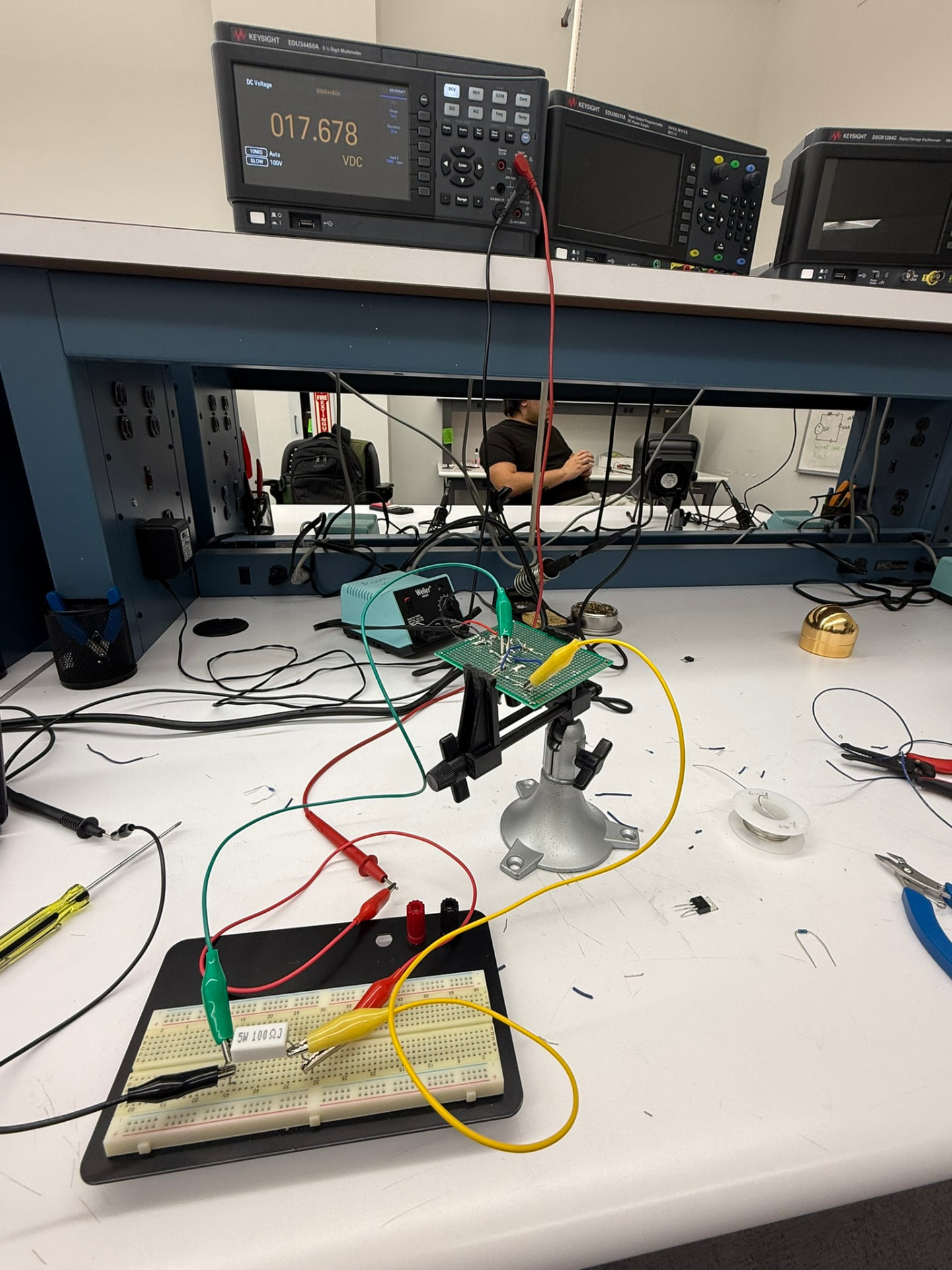
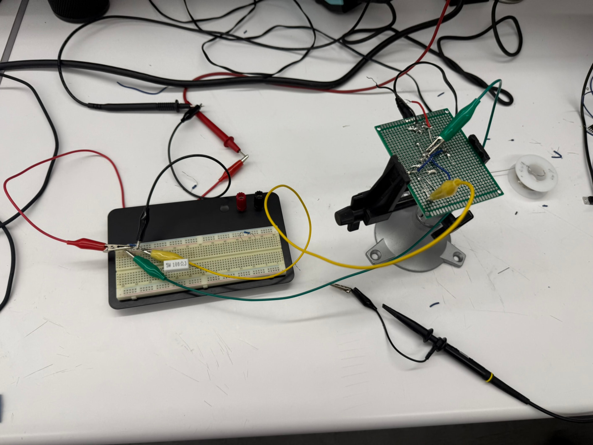
I evaluated the final circuit with a Keysight digital multimeter and oscilloscope, connecting external resistive loads through a breadboard and recording how output voltage and ripple changed as the load drew more current.
At an 18 V unloaded setpoint, the output held up well across three decades of load resistance:
| load | output voltage | peak-to-peak ripple |
|---|---|---|
| 10 kΩ | 17.929 V | 2.225 mV |
| 1 kΩ | 17.587 V | 2.275 mV |
| 100 Ω | 17.256 V | 9.175 mV |
The same pattern held at lower setpoints: at 10 V unloaded, the output ran from 9.562 V at 10 kΩ down to 9.199 V at 100 Ω, and at 5 V unloaded, from 4.952 V down to 4.547 V. The voltage still droops as load current rises — this isn't a perfectly regulated supply — but the source follower keeps the droop to a few hundred millivolts where the potentiometer alone would have lost volts.